XPCB Limited
Tel: +86-755-2301 2705
E-mail: info@apexpcb.com
Add:Building 3, JinFeng Industry Area, Heping Community, Fuyong Town, Baoan District, Shenzhen, 518103, China
The designer is usually under pressure to launch the paperwork and get the versatile circuit into production. There is, however, a lot in danger. Establishing for medium-to-high quantity PCB manufacturing requires significant physical and monetary resources. To avoid potential heat from management, the developer has to insist on PCB prototyping the product as well as a complete style review before release.
DFM Review Criteria
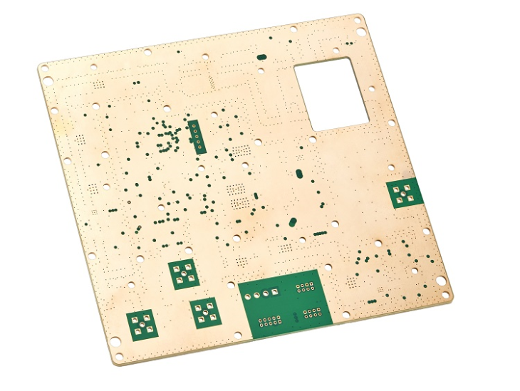
Comprehensive documentation is essential. The intent is to give the fabricator with a breakdown as well as description of the products defined for the flex PCB circuit construction, materials stack-up, reinforced/stiffened areas, essential density areas, and also to define a solder-compatible surface area coating for all element land pattern features. For the much more complex multilayer as well as Rigid Flex PCBapplications include cross-sectional sights. Essential bend or distance places need to be identified with recommendation dimensions as well as it will be handy to provide different sights showing a mounted flex configuration.
The key recommendations for assessing the Flex PCB are tooling holes as well as fiducial targets. Non-plated tooling holes are commonly made use of for maintaining the placement of the circuit throughout singulation and also, when backed with or part of a stiff area, PCB assembly handling. Fiducial attributes ought to be provided in each circuit area or local discontinuation location to provide a monotonous ‘information’ recommendation for a lot more exact element placement. The optimal fiducial is a solid loaded 0.25 to 0.5 mm (.010″ to.020″) size circle. Cover layer material should offer enough clearance to ensure that it does not overlap into the fiducial target attributes throughout the cover layer-to-base circuit lamination experience.
The use of fiducial attributes is a typical technique for:
– Solder stencil x, y as well as theta alignment
– Precise surface place element placement
– Reducing the effects of variable material shrinkage conditions
– Compensation for any kind of random distortions in flex PCB materials
PCB Assembly paperwork will certainly consist of a costs of material, approved vendor list, component referral designators and also any unique requirements. Establish clear, detailed drawings and also PCB Assembly directions. This file ought to include part details and also basic places. The CAD file will provide precise component X-Y collaborates as well as orientation data needed for assembly processing. All SMT tools are straightened as well as put into their particular land patterns utilizing the body center as a recommendation point for placement coordinates. The fiducial targets described above will certainly assist in developing these specific X-Y collaborates for solder printing, component positioning and also orientation. With versatility comes integral dimensional instability about hardboards or solid metal items. When several element placing sites are divided by too much range it is suggested that numerous fiducial functions be offered. Using several datum features is an usual method for minimizing or eliminating the impacts of variable contraction or procedure distortion in flex PCB products. Numerous areas will certainly offer a tighter tolerance within each datum zone or termination location while unwinding the should maintain a limited tolerance of the Flex PCBinterface in between various other termination areas.
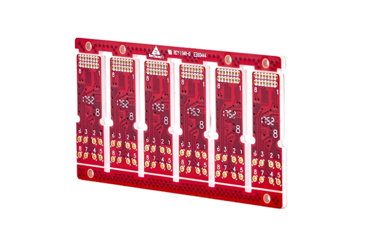
Nesting and also Palletizing
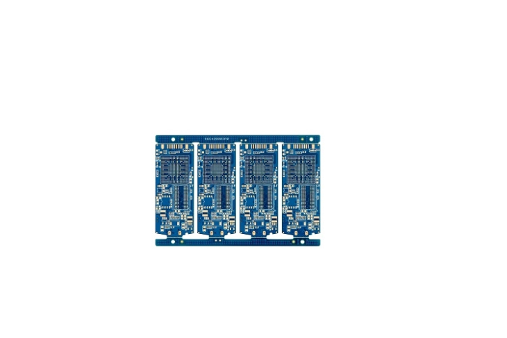
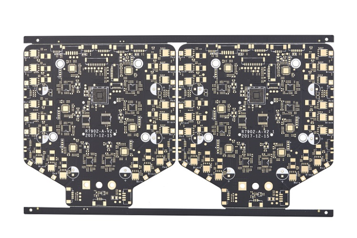
Flex PCB devices can be furnished in panelized layouts. This layout will certainly boost the PCB manufacturing and also assembly process effectiveness as well as optimizing material use. Automated dealing with for in-line assembly handling for Flex PCB equipped with a provisional rigid support as well as multilayer Rigid Flex PCB requires a rather consistent board synopsis.
XPCB Limited
Tel: +86-755-2301 2705
E-mail: info@apexpcb.com
Add: Building 3, JinFeng Industry Area, Heping Community, Fuyong Town, Baoan District, Shenzhen, 518103, China