XPCB Limited
Tel: +86-755-2301 2705
E-mail: info@apexpcb.com
Add:Building 3, JinFeng Industry Area, Heping Community, Fuyong Town, Baoan District, Shenzhen, 518103, China
5 Most Common Flexible Printed Circuit Board Design Errors
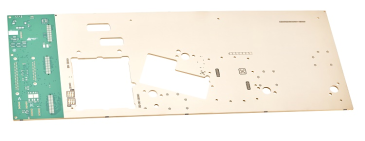
Flexible Printed Circuitry (FPC) offers a significant possibility for the packing engineer as well as digital developer. These functional electronic wiring systems can be formed, bent, twisted as well as folded up right into endless dimensional setups … restricted only by a technician’s origami imagination. Hereof they provide significant design benefits over a two dimensional and also stringent stiff published circuit board (PCB). This added dimension could make flex circuits a developer technician’s desire, however with the enhancement of adaptability come some “guidelines” that should be complied with (sounds like an oxymoron??) to make certain a durable design is attained.
Various manufacturing methods and also material collections are used for FPC’s and an instant distinction is the dimensional residential properties. Rigid published circuits are generally much more dimensionally steady vs. the common polyimide film utilized as the foundation in 98% of the flex circuits produced. This boosted dimensional variability suggests a flexible circuit calls for various design regulations than its stiff printed circuit board relative. Regrettably, much of the design software offered usages stiff PCB design policies and also this can create manufacturing and also practical problems for the versatile circuit. Getting a flexible circuit design ready for fab is referred to some in the industry as “flexizing” the design.
The list below information five of the a lot more typical ways “flexizing” makes a layout more robust, a lot more producible, and prepared for fabrication.
Solder mask or coverfilm openings: During construction adaptable wiring could show dimensional adjustment after exposure to processes like pumice scrubbing, copper plating, and/or etching. While some adjustment can be accounted for, flexible wiring design guidelines normally need bigger tolerances to fit succeeding registrations for coverfilm, supports, or pass away cutting. Extra consideration is required for the glue squeeze out that occurs during lamination of the coverfilm dielectric. Making complex the forecast of compensating layout attributes is the myriad of sequences and experiences required to produce a custom-made adaptable circuit. The bottom line is the openings in the coverfilm normally need to allow even more area in a flex circuit style.
Spacing in between solder pads and also nearby traces: Here is the tradeoff, i.e. style concession, which will certainly be made based on thing # 1. When the coverfilm or soldermask openings are made larger, the edges of the surrounding conductor traces could be revealed if they were routed too close to a solder pad. If solder bridges between connector pins or pads, this could create shorts. Physical dimension of the circuit is an additional element that could affect enrollment ability. As a whole more area is needed in between a solder pad and an adjacent conductive trace to fit the coverfilm or soldermask positioning resistance.
Stress factors in conductors: Because flex wiring is utilized in both fold to mount as well as vibrant bending applications, trace setups that are acceptable in a rigid PCB might create problems in a flexible circuit. Conductor traces with sharp edges and also intense times at the base of solder pads end up being all-natural “tension points” when the location near them is bent. This can lead to trace bone fracture or delamination. A good adaptable circuit design will have a smooth radius for conductor turn points (as opposed to sharp corners) and a gentile radius from the trace to the pad fillet instead of a sharp angle. Discerning add-on of stiffeners will certainly stop flexing in firm regions and also is a typical layout technique.
Stacked traces: Traces on other sides of the dielectric should not straight “stack” on each other. When the circuit is curved if they straight align in parallel with a trace on the other side, traces in stress (on the outside of the bend span) may fracture. The traces in tension are forced further from the neutral axis of the folded area as well as could fracture, particularly with duplicated bending. An excellent design technique is to maintain the copper in the neutral axis of a bend deliberately this area as a solitary conductive layer. When this is not feasible, a proper style will “surprise” the traces between leading and bottom copper layers to prevent top and lower positioning.
Soldered joints as well near to flex factor: A solder joint is formed by an intermetalic bond of the solder alloy to the copper trace. While the copper trace is normally versatile, areas that have been soldered come to be really rigid and also stringent. When the substratum is curved near the side of the solder joint, the solder pad is either going to fracture or flake. Either circumstance will create major functional concerns.
The bottom line is that designing a flex circuit with typical PCB software program can result in some major manufacturability and dependability issues. It is most ideal to work with your flexible circuit vendor or an adaptable circuit style specialist to either “flexize” the style prior to beginning fabrication or create the format straight from a net checklist. This will certainly assure that the style can be manufactured to satisfy your requirements.
XPCB Limited
Tel: +86-755-2301 2705
E-mail: info@apexpcb.com
Add: Building 3, JinFeng Industry Area, Heping Community, Fuyong Town, Baoan District, Shenzhen, 518103, China