XPCB Limited
Tel: +86-755-2301 2705
E-mail: info@apexpcb.com
Add:Building 3, JinFeng Industry Area, Heping Community, Fuyong Town, Baoan District, Shenzhen, 518103, China
What is covered copper?
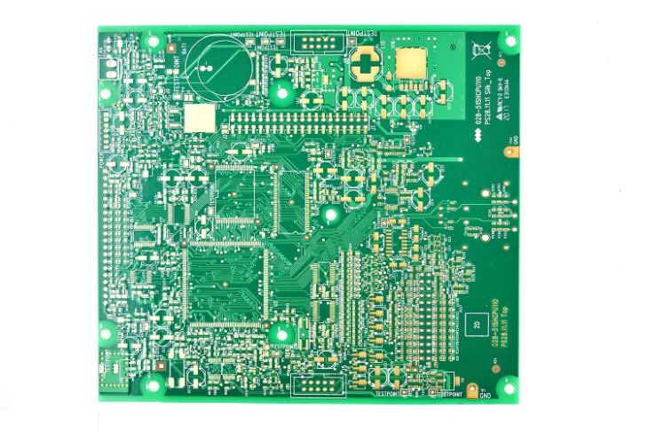
 The covered copper is to use the idle space on the circuit board as the base surface and then fill it with solid copper, which areas are also called copper-pouring. The significance of copper coating lies in: reducing ground impedance, improving anti-interference ability; reducing voltage drop, improving power efficiency; and connecting with ground wire, can also reduce the loop area.
For the purpose of making PCB welding as undeformed as possible, most PCB manufacturers will also ask PCB designers to fill the open area of PCB with copper skin or grid-like ground wire. If the copper coating is not handled properly, it will not be worth the loss. It is well known that at high frequency, the distributed capacitance of the wiring on the PCB will work, and when the length is greater than 1/20 of the corresponding wavelength of the noise frequency, the antenna effect will be produced, and the noise will be emitted outward through the wiring, and if there is a bad ground copper coating in the PCB, the copper coating will become a tool to transmit noise.
Therefore, in the high-frequency circuit, never think that the ground wire is connected somewhere, this is the “ground wire “, must be less than \955;/20 spacing, in the wiring hole, with the multilayer plane” good grounding “. If the copper clad is properly treated, the copper clad not only has the function of increasing the current, but also plays the dual role of shielding interference.
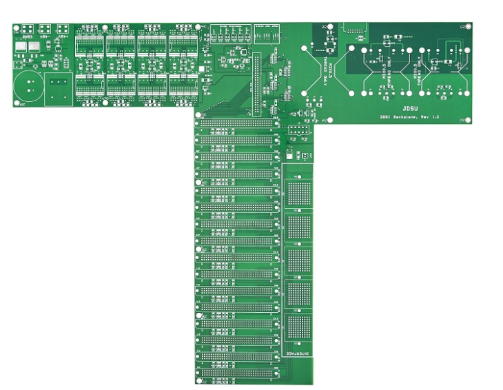
Two forms of copper coating
A large area of copper, with the dual effect of increasing current and shielding, but a large area of copper, if the wave soldering, the board may be warped, or even blister. Therefore, a large area of copper, generally will open a few slots, to relieve copper foil foaming.
 The pure copper mesh is mainly shielded, the effect of increasing the current is reduced, from the point of view of heat dissipation, the grid has advantages (it reduces the heating surface of copper) and plays a certain role of electromagnetic shielding. In particular, for circuits such as touch, as shown below: it is important to note that the grid is made up of interlaced lines, and we know that for circuits, the width of the line has its corresponding “electrical length” for the frequency of the circuit board (see the book for details).
When the working frequency is not very high, perhaps the function of the grid line is not very obvious, once the electric length and the working frequency match, it is very bad, you will find that the circuit is not working properly at all, and the signal of the interference system is transmitted everywhere.
XPCB Limited
Tel: +86-755-2301 2705
E-mail: info@apexpcb.com
Add: Building 3, JinFeng Industry Area, Heping Community, Fuyong Town, Baoan District, Shenzhen, 518103, China