XPCB Limited
Tel: +86-755-2301 2705
E-mail: info@apexpcb.com
Add:Building 3, JinFeng Industry Area, Heping Community, Fuyong Town, Baoan District, Shenzhen, 518103, China
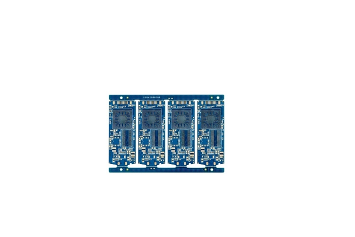
The increase of the winding density certainly represents the need for the enhancement of the thin line technology, and also represents that the ability of the exposure technology to the position must be improved. Because of the increased utilization of the array-type construction products, not only the line and the welding pad, but also most of the green paint to cover the edge of the copper pad to increase the trust of the assembly has a harsh exposure test. At present, the high density multi-layer circuit board green paint cover specification, from 50um unilateral to 10um design have, of course, can be seen that the design density of the structural loading board will be a little higher than the normal circuit board.
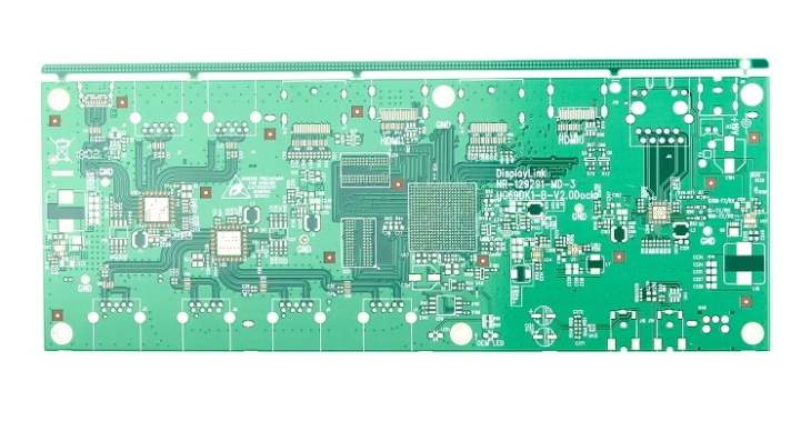
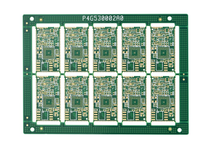
In addition, in the design of some high-density electronic products, because of the demand for modularization, the assembly area of the parts on the surface of the multilayer circuit board is greatly reduced, so some simple passive components will be expected to be made in the way of embedding. This can strive for a larger assembly space from the electrical point of view, for some high-frequency applications also have the function of reducing noise. So there are already some modular products or high-level system products using this design pattern. Figure 10.2 shows an example of the embedded capacitance design for a circuit board for the system.
For the production of meticulous lines. Basically, it’s not just the fineness of the line, but also the stable control of the variation of the line width. At the core of this technique is the use of high resolution image transfer technology. At the same time in the overall production tool system, it is also necessary to adopt a higher size stability design to maintain the coordination of image transfer.
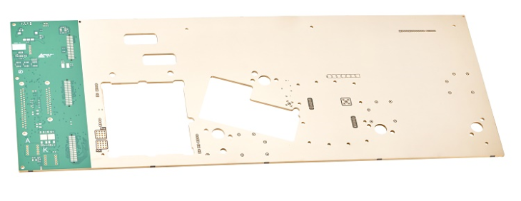
For ultra-fine line making, the so-called thin copper process is a process technology that must be considered. As for the high-layer circuit board which is not recognized as high-density circuit board in general definition, it is also a high-density circuit board in terms of line density per unit area. In order to reduce the thickness of the whole circuit board to reduce the difficulty of making and improve the reliability of the finished product, it is necessary to improve the operation ability of the sequence pressing and the thin inner layer.
The biggest challenge for making such boards is that the lines become so thin that many of the traditional notions that have been examined to repair them no longer exist. Such a concept makes many optical checks a tool for collecting data, but it doesn’t actually help tinkering. Therefore, after product variation, manufacturing management and ideas need to be moderately changed.
In order to make the ultra-fine line, it is easy to make the line by using the way of the electric bottom of the line, but to make the thin line, the photosensitive film will be thinner and thinner, which makes the technology of line electroplating especially important in the making of some thin lines. Because of this, there are different electroplating systems, among which the insoluble anode, vertical walking electroplating line design, such a design to improve the uniformity of the circuit and the stability of the solution, there are many new lines to use this design for production.
As for the most difficult area of exposure, the exposure of green paint is the most, the exposure resolution here is not easy to reach a high level, plus the circuit board after a long journey to the process, the size of the stability has been produced variation, so it is difficult to do a good job of exposure to the position. At present, for some products beyond the ability of alignment, if typesetting allows for regional sub-exposure, some exposure machines have been produced in this way.
XPCB Limited
Tel: +86-755-2301 2705
E-mail: info@apexpcb.com
Add: Building 3, JinFeng Industry Area, Heping Community, Fuyong Town, Baoan District, Shenzhen, 518103, China