XPCB Limited
Tel: +86-755-2301 2705
E-mail: info@apexpcb.com
Add:Building 3, JinFeng Industry Area, Heping Community, Fuyong Town, Baoan District, Shenzhen, 518103, China
Abstract
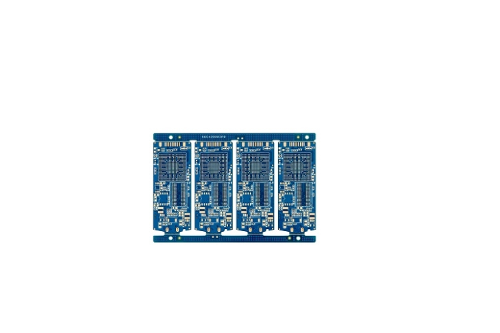
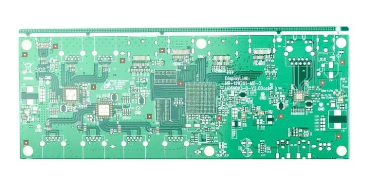
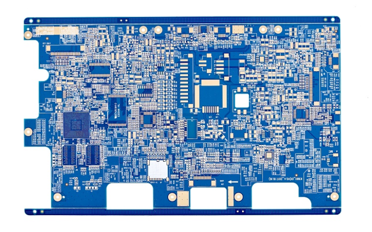
Electronics tend to be thin in thickness, small in size and light in weight, with more functionality and speed. Therefore, the electronic industry has developed diversified and advanced technologies and methods to enable it to increase the density, quantity and variety of integrated circuits (IC) on the same circuit board.
The way to increase the density of packages and connections is from the evolution of through-hole technology(PTH) towards the surface assembly technology(SMT), which leads to the further application of Wire bonding. The reduced connection line spacing and application of chip size packaging technology (CPS) increase the density of the device. thus derived a new surface treatment process, ENEPIG. The ENEPIG’s process and advantages will be described below.
Key words
Ni/Pd/Au、ENEPIG、Wire bonding、Black PAD
Introduction of ENEPIG Process
Chemical nickel palladium gold is a layer of palladium between nickel and gold, which can prevent the corrosion caused by the displacement reaction and prepare for the sinking gold. Gold is tightly covered in palladium, providing a good contact surface.
Process:

Chemical reaction mechanism

Picture from network
The characteristic chemical Pd(No electrolytic palladium)
Performance comparison of different surface treatments

★The more stars the better
The image of palladium layer layer

The Advantages of ENEPIG
XPCB Limited
Tel: +86-755-2301 2705
E-mail: info@apexpcb.com
Add: Building 3, JinFeng Industry Area, Heping Community, Fuyong Town, Baoan District, Shenzhen, 518103, China