XPCB Limited
Tel: +86-755-2301 2705
E-mail: info@apexpcb.com
Add:Building 3, JinFeng Industry Area, Heping Community, Fuyong Town, Baoan District, Shenzhen, 518103, China

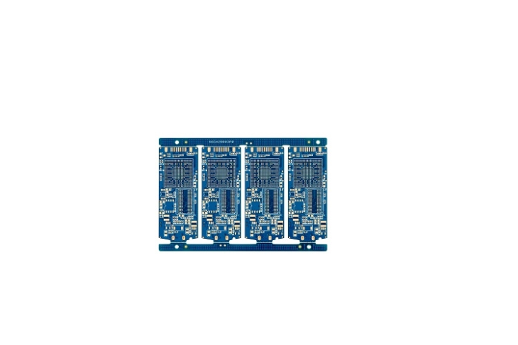
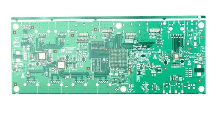
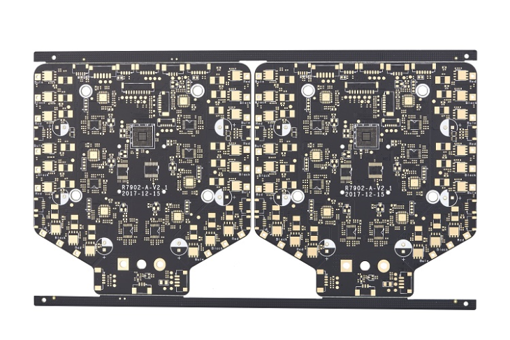
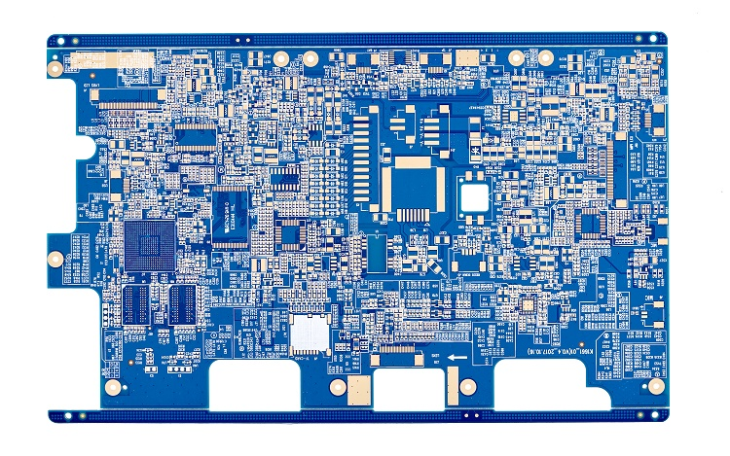
Electronic products have become an indispensable part of our daily life. At the heart of these electronic devices, from smartphones to electric cars, are printed circuit boards (PCBS). Most people will recognize them when they see printed circuit boards, which are small green sheets of copper wire covered with parts. If you’re interested, you can take the electronics apart and see the printed circuit boards.

The printed circuit boards are made of fiberglass, copper foil, and other metal parts that are held together by epoxy resin and insulated with a resistance layer. The color we see on the surface of the circuit board comes from the color of the solder film.

I don’t know if you’ve noticed anything that’s stuck to the surface of the circuit board, but don’t think it’s just decoration. An advanced circuit board that does not have high-quality components sticking to the surface of the circuit board accurately will not provide the corresponding function in any way. Printed circuit boards with components are called assembled circuit boards (assembled PCB), and the manufacturing process is called printed circuit board assembly or PCBA. In contrast, printed circuit boards that do not have electronic components on their surfaces are called bare boards. The copper wires on the bare board, called wires, electrically connect the connectors to the electronics and ultimately allow the circuit board to work and operate in a specially designed manner.
So how are these assembled printed circuit boards made? PCBA is a simple and complex process. It is simple because it consists of only a few automatic and manual steps, and the whole process is simple. It’s complicated because every step is so critical that even a small deviation can lead to disastrous results. As modern electronics move toward miniaturization, each step of the assembly process requires more detail. To help you better understand the PCB assembly process, we will explain the operation of each step in detail in this article for your reference.
There are two main types of modern PCB assembly technologies: surface mount technology (SMT) and through hole (THT).
● surface mount technology
Surface mount technology is mainly used in the assembly of sensitive components, some very small resistors or diodes, etc., through the surface mount technology, these components are automatically placed on the surface of the circuit board, known as surface mount devices. Surface mount technology can be applied to small-sized components and integrated circuits (IC). For example, in XPCB, the smallest component package we can mount is 01005, which is smaller than the tip of a pencil.

● through-hole technology
The through-hole technique is suitable for components with wires or pins that must be installed on the circuit board by inserting them into holes in the circuit board. Additional leads must be welded to the other side of the circuit board. Through-hole technology is used for assembling circuit boards containing large components, such as capacitors.

Due to the differences between surface mount and through-hole techniques, they also have to go through different assembly processes. Next, this article introduces the PCBA assembly process in combination with two different assembly technologies.
It is necessary to do some preparatory work before the PCBA can be formally started, which helps circuit board manufacturers to evaluate the function of circuit board design, mainly reflected in the aspect of manufactory design (DFM) inspection.
Most companies that specialize in circuit board assembly require circuit board design documentation and any other design instructions and specific assembly requirements. This is because circuit board assembly companies can check the circuit board design documentation for problems that may affect the function or manufacturability of the circuit board, which is what manufacturability design inspection is all about.
Manufacturability design inspection looks at all design specifications for circuit boards. Specifically, this check looks for any missing, redundant, or potentially problematic functionality. Any of these problems can seriously affect the realization of the final project functionality. For example, if the spacing between circuit board components is too small, the product may be short-circuited or even scrapped.
By identifying potential problems before production can proceed, manufacturability design checks can reduce manufacturing costs and eliminate unforeseen expenses because they reduce the number of scrapped circuit boards. XPCB provides free inspection of manufacturability design, saving cost for customers, ensuring product quality and pass rate.
The first step in SMT assembly is to apply the solder paste evenly to the circuit board, specifically to the pads of the components.The precise coating benefits from the stainless steel mesh, which has precise holes according to the circuit board design document.When the solder paste is printed, the solder paste will be accurately coated on the solder pad.The blade pressure, blade Angle and blade speed is to test the circuit board assembly manufacturers technology and experience. Once any link is handled improperly, solder paste printing cannot be considered a success.

The paste itself is a gray metallic substance, made up of tiny balls of metal, also known as solder. The tiny spheres are made up of 96.5% tin, 3% silver and 0.5% copper.Solder paste mixes solder with flux, a chemical design that helps solder melt and bond to the surface.
In the professional PCB assembly line, first, the mechanical fixture will be the circuit board and steel mesh fixed in place; Then the applicator places the solder paste exactly on the predetermined area. Next, the machine will solder paste on the steel network, evenly coated in each open area; Finally, when the mesh is removed, the solder paste is left in place.
After the solder paste is printed, the conveyor moves the circuit board to the pickup machine, which places the surface mounted devices (SMD) on the printed solder paste circuit board.
In the past, this was a manual process that required tweezers, with assemblers picking up and placing components manually. Today, with advances in technology and the trend toward smaller electronics, this process has become automated, which has greatly improved assembly efficiency and accuracy.
The pickup and placing machine picks up the circuit board with a vacuum clamp and moves it to the pickup and release position to pick up and place the material.The machine then locates the circuit board on the stage, and the components are then placed on top of the solder paste in the pre-programmed position.

Once the solder paste and surface-mount components are in place, it is time to secure them to the circuit board. Circuit board assembly achieves this through a process called “reflow”, in which the solder paste is melted at high temperature, cooled and cured permanently so that the surface-mount elements are fixed to the circuit board surface.
After the pick and place process, the circuit board is moved by a conveyor belt to a large reflow furnace, which consists of a series of heaters that gradually heat the circuit board to 250 degrees Celsius, which is high enough to melt the solder in the paste.
Once the solder melts, the circuit board continues to move through the entire reflow furnace. The molten solder is then cooled and solidified in a controlled manner by a series of cooler heaters, creating a permanent solder spot that connects the surface-mount elements to the circuit board.
Many assembled circuit boards require special consideration during reflow, especially double-sided circuit board assembly. Double-sided PCB assemblies require each side to be individually printed and reflowed. First, one side with less and smaller parts is printed, picked up and returned through the mesh, and then the other side goes through the same process.
Once the surface-mount components are in place after reflow soldering, this does not mean that the circuit board assembly is complete. The assembled circuit board needs to be functionally tested. Usually, movement during reflow can result in poor solder joint quality or a complete lack of connection, or even a short circuit.
Common methods for checking for these errors and dislocations include:
☆ manual inspection
Although automation and intelligent production are predictable trends, the PCB assembly process still relies to some extent on traditional manual inspection. For small batches of assembled circuit boards, visual inspection is an effective method to ensure the quality of the boards after reflow soldering. However, as the number of circuit boards to be tested increases, this approach becomes increasingly impractical and inaccurate. Furthermore, observing small materials for more than an hour can lead to optical fatigue, resulting in inaccurate inspection results.
☆ automatic optical detection (AOI)
Automatic optical detection is a suitable detection method for assembling circuit boards in larger quantities. The automatic optical detector, also known as AOI, relies on a series of high-performance cameras that are arranged at different angles to see the quality of the solder joints.Solder joints of different quality reflect light in different ways, scan the circuit board, collect images, and then compare the collected data with the data entered into the instrument to identify the quality of the solder joints.The AOI performs this task at a very high speed, enabling it to process a large number of circuit boards in a relatively short period of time.
☆ X-ray detection
X-ray detection is another method of detecting assembled circuit boards, most commonly used for more complex or layered circuit boards.X-rays can be viewed through the layers to identify any potential hidden risks.
Regardless of the method used, the next step in the process is to test the part to ensure that it performs its relevant functions and performance. This involves testing the quality of the printed circuit board connections, which require more steps to test the correct function if the board is programmed or calibrated.
These checks can be carried out periodically after the backflow process to identify any potential problems and risks. These periodic inspections ensure that errors are detected and fixed as quickly as possible, which helps manufacturers and designers save time, manpower, and material costs.
☆ final inspection and functional testing
After the welding step in the PCBA is completed, the final inspection will test the function of the assembled circuit board. This inspection is called a “functional test”.This test mainly determines whether the performance of the circuit board meets the requirements by simulating the operation of the circuit board in the final application. In this test, the power and analog signals are run through the circuit board, and the tester monitors the electrical characteristics of the circuit board.
If these characteristics (including voltage, current, or signal output) manifest unacceptable fluctuations or peak outside a predetermined range, the circuit board fails the test.
Functional testing is the last and most important step in the PCB assembly process, because it determines the success or failure of all previous assembly steps and is why regular testing and inspection throughout the assembly process is so important.
Printed circuit board THT (through-hole Technology) assembly is a traditional assembly method of circuit board. Unlike SMT assembly, which relies entirely on automatic procedures, the through-hole assembly process includes both manual and automatic procedures.
This step is done manually by a professional engineer. The engineer needs to quickly and accurately place the electronic components in the appropriate location according to the customer’s PCB design document.The plug-in must comply with the requirements and operating standards of the through-hole installation process to ensure the high quality of the end product. For example, components must have the correct polarity and direction, prevent crosstalk between components, make the finished component mount to the appropriate standards, and wear anti-static wristbands when dealing with electrostatic sensitive components such as IC.
Once the plug-in is complete, the circuit board is placed in a matching shipping frame, where the circuit board inserted into the material is automatically checked to see if the material is placed correctly. If problems with component mount are observed, it is easy to correct them immediately. After all, this was done before welding.
After the material is properly inserted into the circuit board, the through-hole components are welded to the circuit board. In the THT assembly process, wave soldering is used to complete the welding process. In a wave soldering system, the circuit board moves slowly through a wave of liquid solder at a temperature of approximately 500°F. After that, all wire or wire connections can be successfully obtained so that the through hole assembly is securely attached to the circuit board.
The next step is the same as the SMT assembly process, the THT assembly welded circuit board also needs to be inspected and tested to ensure its accurate performance and high quality.
When you hold a new assembled circuit board in your hand, you will be amazed by its clean, smooth and free from impurities, but in fact, the circuit board assembly process can be a dirty looking process. The solder paste is printed with a certain amount of flux, and production line workers may transfer grease and dirt from fingerprints and clothing to the surface of the PCB. Therefore, the finished circuit board involves both the aesthetics and the actual situation.
If the flux is not cleaned in a timely manner, the flux residue will become sticky after being left on the PCB surface for a few months and will also become acidic, damaging the solder joints over time.In addition, customer satisfaction is often affected when residue and fingerprints are applied to the surface of a new circuit board. Therefore, it is very important to clean the circuit board after welding.
XPCB will clean all the circuit boards that are about to leave the factory. Stainless steel high-pressure cleaning equipment using deionized water is the best tool for removing circuit board residues. Cleaning printed circuit boards in deionized water poses no threat to equipment because ions in conventional water damage the circuit, not the water itself. Therefore, deionized water is not harmful to PCB during the circuit board washing cycle.
After cleaning, use compressed air for a quick drying cycle to prepare the completed PCB for packaging and transportation.
If you have any questions about PCB or PCBA, please leave us a message.
If you need EMS for any project, please contact us.
XPCB Limited
Tel: +86-755-2301 2705
e-mail: xpcb02@x-pcb.com
Add: Building 3, JinFeng Industry Area, Heping Community, Fuyong Town, Baoan District, Shenzhen, 518103, China
XPCB Limited
Tel: +86-755-2301 2705
E-mail: info@apexpcb.com
Add: Building 3, JinFeng Industry Area, Heping Community, Fuyong Town, Baoan District, Shenzhen, 518103, China