XPCB Limited
Tel: +86-755-2301 2705
E-mail: info@apexpcb.com
Add:Building 3, JinFeng Industry Area, Heping Community, Fuyong Town, Baoan District, Shenzhen, 518103, China
OREWORD
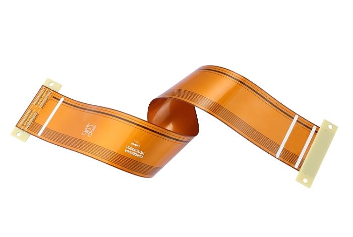
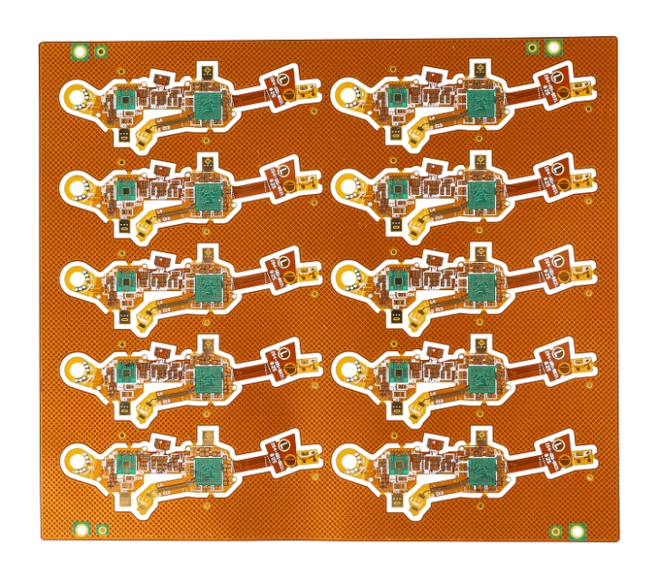
As a special interconnection technology, rigid-flex multilateralism printed board has been widely used in computer, avionics and military electronic equipment, but it also has the disadvantages of high technology, high production cost and difficult to change and repair.

Rigid-Flex Circuits Process Characteristics
1.Actualize 3D stereo wiring assembly
2.It can be used dynamically to meet the demand of high flexible
3.High-density circuit design
4.High reliability,low impedance loss,complete signal transmission
5.Shorten installation time,reduce installation cost,easy to operate.
6.Having rigid plate hardness and supporting function.
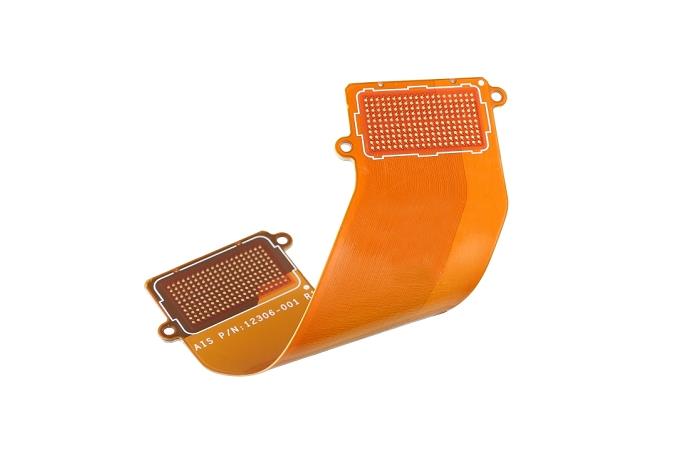
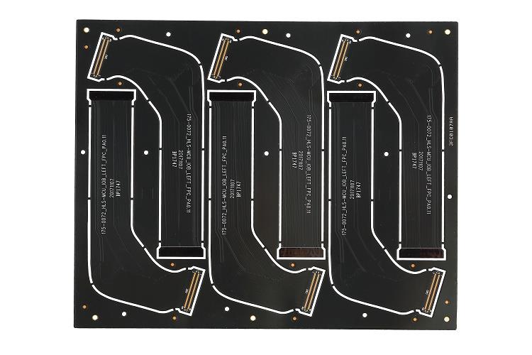
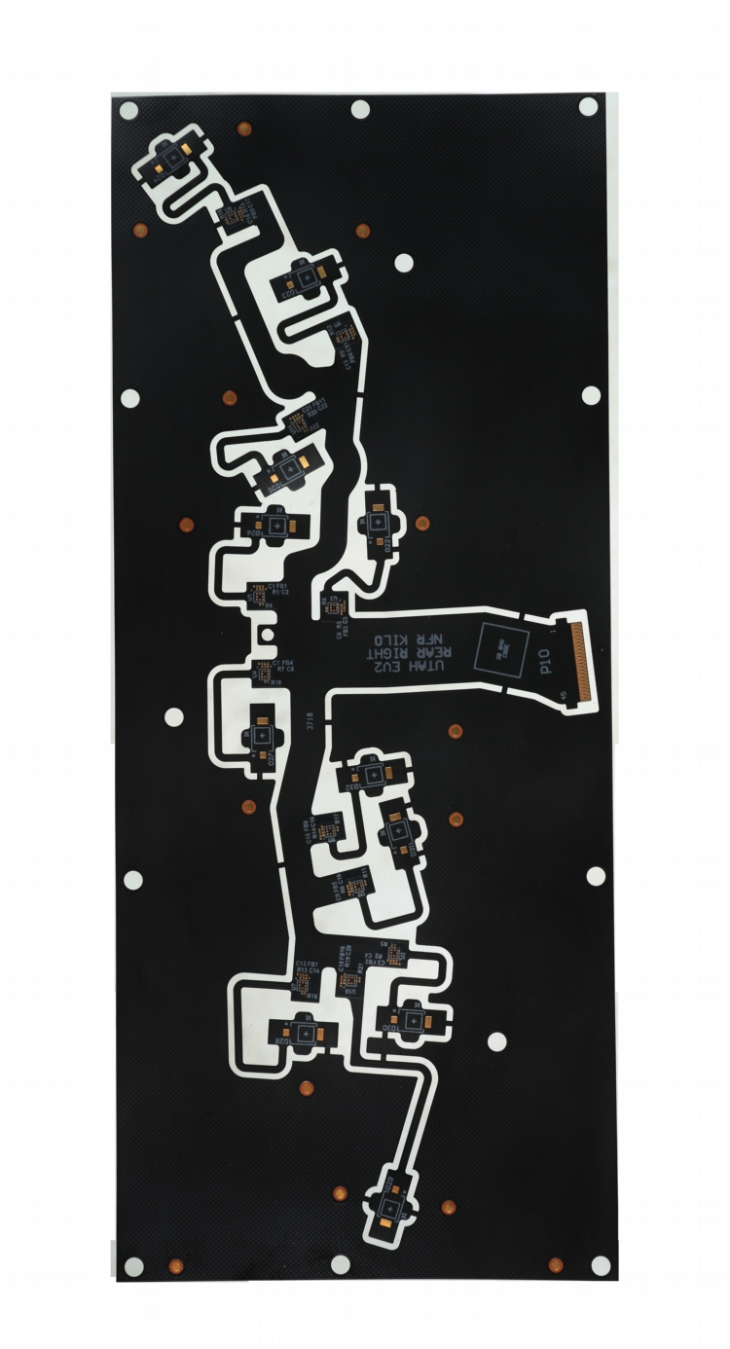
Laminated Stack-ups
The rigid-flex circuits stack-ups are diverse, consisting of one or more flexible materials and one or more rigid materials, which are electrically interconnected by drilling, coating and laminating processes. According to the requirements of the components, they can be designed into one or more flexible and rigid zones.
Stack-up1 Inner Flex circuits symmetrical structure
 1.The flex in middle layer,also designed 1-3 FCCL(Double side)
2.If there are more than one FCCL, it is mostly use adhesive to laminated considering the flexible.
3.Use one or more core boards (copper foil) for the outer layer ,Top and Bot core has the same thickness of FR4.
4.The flex layer and the core layer are mostly use no-flow PP for filling, bonding force and glue overflow consideration, and the core layer and the core layer are only for filling and bonding, mostly normal PP.
Stack-up2 Flex area designed gold finger
1.Commonly seen with plug finger with PI reinforcement, press finger with SUS or FR4 reinforcement.
2.The stiffer can be designed on top or bot layer.
Stack-up3 N-Rank HDI
HDI Rigid-Flex board is usually 1-3-rank,2-3 times pressure design, mostly 6-12 layers, the thickness of the board is above 0.5 mm,also has buried holes.But in some precision instruments or consumer electronics (such as blue-tooth headphones), the requirements of the structure thickness is usually between 0.3-0.4, in the process need to use etching open cover or PI film to assist open cover.

Stack-up4 Flex area has air-gap
1.For the multi layer flex need design circuits and need well flexible, the gap structure will be designed.
2.Do not design conduction holes in gap area.
3.Design attention should not be in the gap area design conduction hole, the number of common air gap in 1-3, soft plate may only use thin copper and thin cover film, to reduce the soft and hard junction bulge, to ensure that the plate flat, to avoid drilling peak phenomenon.
Stack-up5 TOP and BOT asymmetric structures
1.The Flex layer is in the outer layer, the surface covering film is ntolerant to strong alkali, therefore the partial treatment will cause the covering film atomization, therefore does not allow the post-roasted plate rework, also may not open the ultrasonic wave and the grinding brush in the copper plating process.
2.The upper and lower asymmetry should pay attention to the problem of plate warping caused by the inconsistency of the upper and lower stress after pressing or baking, which can be controlled by adjusting the upper and lower residual copper rate, the direction of the splicing plate and the slotted edge of the plate.
Stack-up6 Other more complex stacks

These structures are designed to meet customer needs .For example, in the second picture, there are two kinds of thickness in the rigid part of the same board;The thickness of the rigid area in the fourth picture can be much thinner.
XPCB Limited
Tel: +86-755-2301 2705
E-mail: info@apexpcb.com
Add: Building 3, JinFeng Industry Area, Heping Community, Fuyong Town, Baoan District, Shenzhen, 518103, China