XPCB Limited
Tel: +86-755-2301 2705
E-mail: info@apexpcb.com
Add:Building 3, JinFeng Industry Area, Heping Community, Fuyong Town, Baoan District, Shenzhen, 518103, China
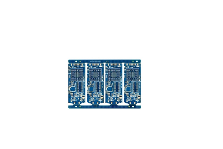
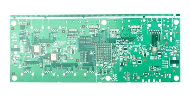
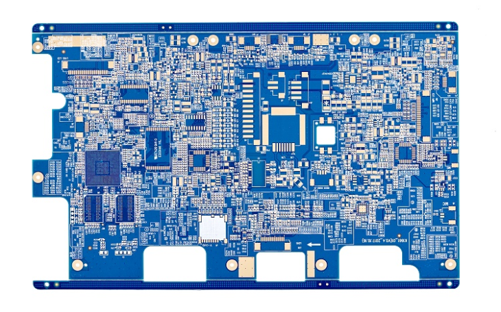
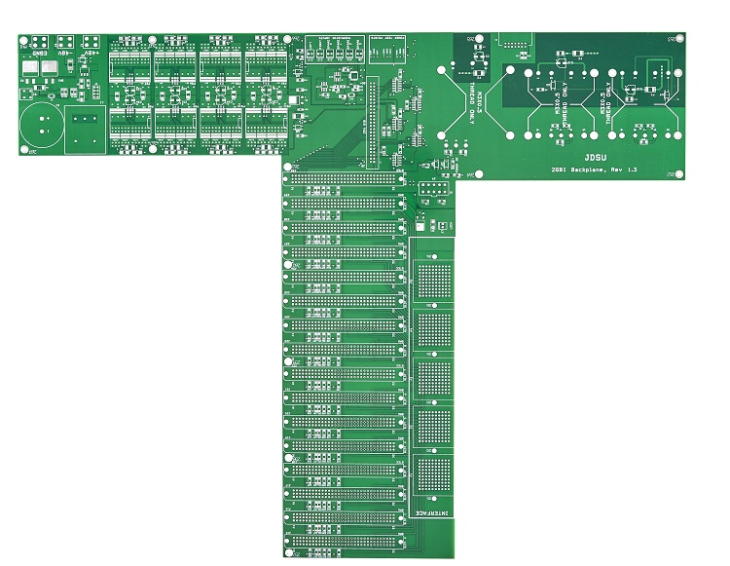
The design of printed circuit board is based on circuit schematic diagram to realize the function required by circuit designers. The design of printed circuit board mainly refers to the layout design, which needs to consider the arrangement of external connection, the optimal layout of internal electronic components, the optimal layout of metal connection and through hole, electromagnetic protection, thermal dissipation and other factors. Excellent layout design can save production costs, achieve good circuit performance and heat dissipation performance. Simple layout design can be achieved by hand, complex layout design needs to be achieved with the help of Computer Aided design (CAD).

XPCB Limited
Tel: +86-755-2301 2705
E-mail: info@apexpcb.com
Add: Building 3, JinFeng Industry Area, Heping Community, Fuyong Town, Baoan District, Shenzhen, 518103, China