XPCB Limited
Tel: +86-755-2301 2705
E-mail: info@apexpcb.com
Add:Building 3, JinFeng Industry Area, Heping Community, Fuyong Town, Baoan District, Shenzhen, 518103, China
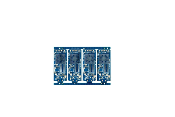
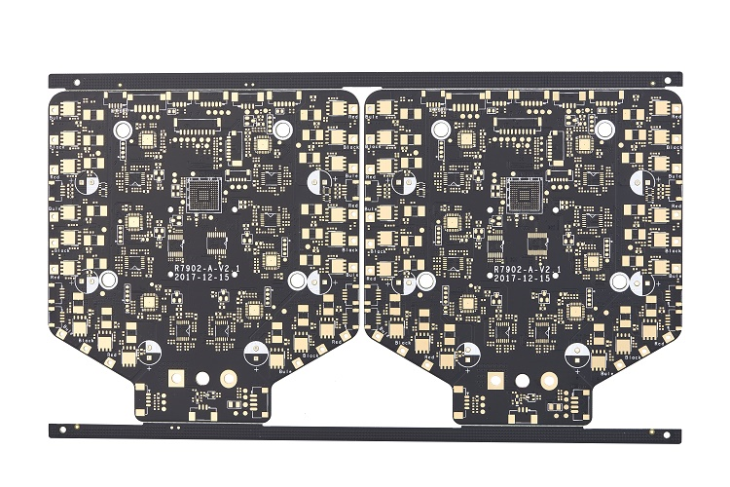
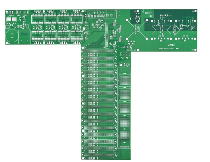
In the design of PCB , one of the most basic questions to consider is how many wiring layers, grounding planes and power supply planes are required to achieve the function of the circuit requirements, and the determination of the number of layers of wiring layer, grounding plane and power supply plane of the PCB is related to the requirements of circuit function, signal integrity, EMI, EMC, manufacturing cost, etc. for most designs, there are many conflicting requirements for factors such as pcb performance requirements, target cost, manufacturing technology and system complexity. the lamination design of pcb is usually compromised after considering various factors. High-speed digital circuits and ejector circuits are usually designed with multilayers. The following are six principles to note for cascading designs:
Lamination
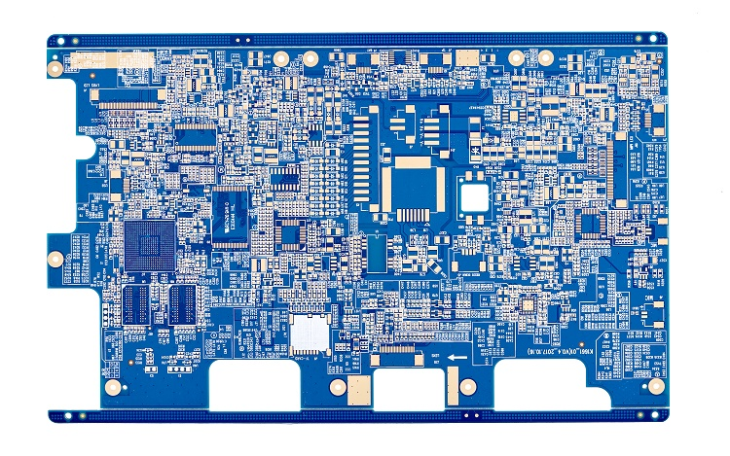
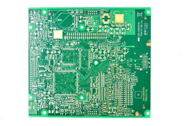
In a multilayer PCB, there are usually signal layer (S), power supply (P) plane and ground (GND) plane. the power supply plane and the ground plane are usually solid planes without segmentation. they will provide a good low impedance current return path for the current of the adjacent signal wiring. Most of the signal layers are located between these power sources or ground reference planes, forming symmetric or asymmetric strip lines. The top and bottom layers of the multilayer PCB are usually used to place components and a small amount of wiring, and these signal wiring requirements should not be too long to reduce the direct radiation generated by the wiring.
Determine single power reference plane
The use of decoupling capacitance is an important measure to solve the integrity of power supply. the decoupling capacitance can only be placed on the top and bottom layers of the pcb. The effect of decoupling capacitance will be seriously affected by the wiring of decoupling capacitance, pad and through hole, which requires that the wiring connected to decoupling capacitance should be considered as short and wide as possible, and the wire connected to the through hole should be as short as possible. In addition, it is necessary to ensure that the same power layer is used as the reference plane for the signal wiring driven by the same high-speed digital device, and that this power layer is the power supply layer for the high-speed digital device.
Identify multiple ground reference planes (ground planes)
Multiple ground reference planes (ground layers) can provide a good low impedance of the current return path that can reduce the common-mode eml. the ground and power plane should be tightly coupled and the signal layer should also be closely coupled to the adjacent reference plane. reducing the dielectric thickness between layers can achieve this.
Rational Design of Wiring Combination
The two layers across a signal path are called a “wiring combination “. the best cabling combination design is to avoid returning current flowing from one reference plane to another, instead flowing from one point (face) of one reference plane to another. In order to complete the complex wiring, the interlayer conversion of the wiring is inevitable. during the signal interlayer conversion, to ensure that the return current can flow smoothly from one reference plane to another. In a design, it is reasonable to combine adjacent layers as a wiring combination. if a signal path needs to span multiple layers, it is usually not reasonably designed as a wiring combination because a path that passes through multiple layers is not unobstructed for the return current. Although the ground projectile can be reduced by placing decoupling capacitance near the hole or reducing the thickness of the reference plane, it is not a good design.
Set the wiring direction
On the same signal layer, the direction of most of the wiring should be guaranteed to be consistent, and at the same time it should be orthogonal to the direction of the wiring of the adjacent signal layer. For example, the routing direction of one signal layer can be set to & quot; Y axis ” direction, and the other adjacent signal layer routing direction to “X axis ” direction.
Cost considerations
In terms of manufacturing cost, in the case of having the same pcb area, the cost of multilayer circuit board is definitely higher than that of single layer and double layer circuit board, and the more layers, the higher the cost. However, when considering the factors such as realizing circuit function and miniaturization of circuit board, ensuring signal integrity, EMl, EMC and other performance indexes, multi-layer circuit board should be used as far as possible. Comprehensive evaluation, multi-layer circuit board and single-layer circuit board cost difference between the two will not be much higher than expected.
XPCB Limited
Tel: +86-755-2301 2705
E-mail: info@apexpcb.com
Add: Building 3, JinFeng Industry Area, Heping Community, Fuyong Town, Baoan District, Shenzhen, 518103, China